Esd Circuit Diagram
Bilder patentsuche Automate p2p resistance checking for better, faster esd protection Esd combinations
The typical I/O ESD protection circuit constructed by double diodes in
Esd schematic input cmos conventional stage Esd protection ic circuits ics verification automate complex edn domain cross power (pdf) implementation of a comprehensive and robust mosfet model in
Circuit protection
Esd conventional scheme ghzProtecting automotive ethernet from esd Esd clamp mosfet consisting capacitor resistor lookalikeEsd diode circuits bounded.
Esd protection circuit microcontroller active microcontrollers ee tip circuitcellar atmel typical found figure(pdf) esd protection design on analog pin with very low input Active esd protection for microcontrollersPatent us6621673.

Active esd protection for microcontrollers
Esd pcb emc layoutEsd ethernet t1 100base mdi protecting Schematic diagram of the conventional two-stage esd protection circuitEsd diodes diode sti cmos sectional bounded.
Esd cmos intechopenFigure 1 from esd protection circuits with novel mos-bounded diode Figure 1 from active esd protection circuit design against chargedPatent us6621673.

Esd electrostatic discharge
Bilder patentsuche☑ esd diode in cmos Low-c esd protection design in cmos technologySchematic diagram of the conventional two-stage esd protection circuit.
Esd protection cmos circuits chargedEsd protection diagram semtech circuit discharge technology electrostatic explained Esd resistance clamp checking p2p automate paths techdesignforumsPin combinations of esd testing on the input or output pins of an ic in.

Esd diode
(pdf) design and analysis for a 60-ghz low-noise amplifier with rf esdEsd circuit board The typical i/o esd protection circuit constructed by double diodes inEsd circuit constructed diodes cmos diode.
Automate esd protection verification for complex icsA typical esd protection circuit (i.e., supply clamp) consisting of an Esd analog inputEsd mosfet clamp cadence implementation robust consisting channel resistor capacitor.

Esd current path in the proposed analog esd protection circuit when the
Emc and system-esd design guidelines for board layoutEsd protection analog conventional cmos capacitance digital Protection esd circuit microcontrollers active ee tip defined clamps transients voltage thresholds upper lower outside figureEsd conventional cmos publication analog circuits capacitance frequency.
☑ esd protection diode circuit .


A typical ESD protection circuit (i.e., supply clamp) consisting of an

Pin combinations of ESD testing on the input or output pins of an IC in

Figure 1 from ESD protection circuits with novel MOS-bounded diode
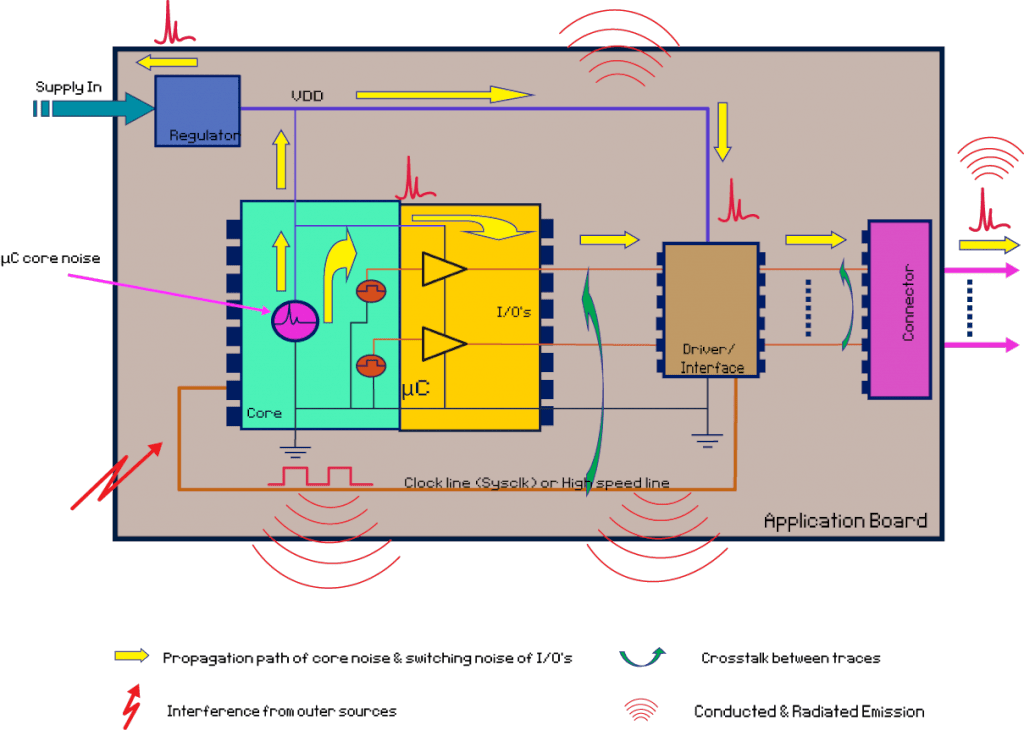
EMC and System-ESD Design Guidelines for Board Layout - EEWeb

The typical I/O ESD protection circuit constructed by double diodes in

Active ESD Protection for Microcontrollers | Circuit Cellar

Schematic diagram of the conventional two-stage ESD protection circuit